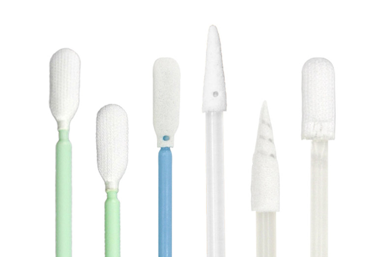
Cleanroom swabs play a crucial role in maintaining the cleanliness and efficiency of semiconductor industry cleanrooms. Diese Spezialwerkzeuge wurden entwickelt, um Verunreinigungen effektiv von kritischen Oberflächen zu entfernen, ensuring the reliable functioning of delicate equipment and the production of high-quality semiconductor devices. In diesem Artikel, we will explore the significance of cleanroom swabs and how they contribute to the success of the semiconductor industry.

Cleanrooms in the semiconductor industry require an environment with extremely low levels of particulate and chemical contaminants. Even the tiniest speck of dust or residue can lead to defects in the final products, resulting in decreased yield and compromised performance. Reinraumtupfer, consisting of a handle and a lint-free, low-particulate swab tip, are specifically designed to eliminate these impurities without leaving any residue behind.
One of the primary uses of cleanroom swabs is the cleaning of sensitive components, such as integrated circuits and microchips. These tiny devices are highly susceptible to damage caused by environmental contaminants. Cleanroom swabs provide a gentle and precise cleaning method, ensuring that no foreign particles or oils are left on the surfaces. By effectively eliminating contaminants, cleanroom swabs contribute to the overall quality and reliability of semiconductor devices.
Moreover, cleanroom swabs are also utilized in the maintenance and cleaning of cleanroom equipment. Semiconductor manufacturing equipment, including deposition systems, etching tools, and lithography machines, must be regularly cleaned to prevent cross-contamination and ensure optimal performance. Cleanroom swabs enable technicians to access hard-to-reach areas and remove any residues or particles that may hinder the equipment’s functionality.
In addition to cleaning, cleanroom swabs are crucial in the validation and monitoring processes within semiconductor cleanrooms. Regular swabbing of critical surfaces allows for the collection of samples to assess the level of cleanliness. These samples are then analyzed to determine the presence of contaminants, ensuring that the cleanroom environment meets the required standards. Cleanroom swabs provide a reliable and convenient method for conducting these essential cleanliness checks.
When selecting cleanroom swabs for use in semiconductor cleanrooms, it is vital to choose swabs that comply with industry standards. Swabs made of high-quality materials, such as polyester or microfiber, are preferred due to their low particulate generation and excellent absorption capabilities. Zusätzlich, swabs with low ionic contamination are essential to prevent any adverse effects on the sensitive semiconductor devices.
Abschließend, cleanroom swabs play a vital role in maintaining the cleanliness and integrity of semiconductor industry cleanrooms. These specialized tools enable the effective removal of contaminants from critical surfaces, ensuring the production of high-quality semiconductor devices. Whether used for cleaning sensitive components or validating cleanliness levels, cleanroom swabs are indispensable in the semiconductor industry’s quest for excellence.
 Reinraum-Schaumtupfer, Polyester-Tupfer, Hersteller von Druckerreinigungskits – MediTech